The Application of Ultrasonic Atomization Spraying Technology in The Electronics Industry
Ultrasonic atomization spraying technology is playing an increasingly crucial role in the electronics industry due to its core advantages of high precision, high uniformity, and high material utilization. It provides a novel solution to many challenges that traditional spraying processes struggle with by atomizing liquid into micron-sized uniform droplets and then precisely depositing them onto the target surface. This technology is widely used in the manufacturing of numerous electronic components, from microscopic semiconductor chips to macroscopic circuit boards.
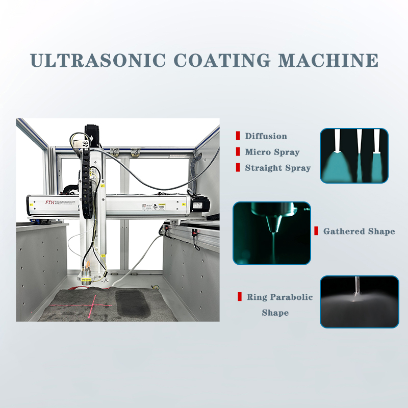
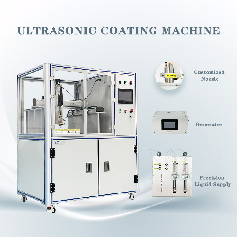
Core Technology Principle: The core of ultrasonic atomization spraying lies in its unique atomization method. The system converts high-frequency electrical energy into mechanical energy through a piezoelectric transducer, generating high-frequency longitudinal vibration. This vibrational energy forms standing waves in the liquid film on the nozzle surface, "breaking" the liquid into micron-sized droplets with a highly concentrated size distribution. Unlike spraying methods that rely on high-speed airflow or high pressure, this process is very gentle. The resulting droplets are then guided to the target substrate by a low-pressure carrier gas, thus achieving precise, controllable, and repeatable coating.
Core Application Areas in the Electronics Industry: The application of ultrasonic spraying technology in the electronics industry has covered several key areas.
Semiconductor and Microelectronics Manufacturing
In the semiconductor and microelectronics fields, as device sizes continue to shrink and structures become increasingly complex (such as MEMS devices), traditional methods like spin coating are proving inadequate for covering trenches and three-dimensional microstructures with high aspect ratios. Ultrasonic spraying technology, with its unique advantages, has become a key process for solving these challenges.
Photoresist Coating: This is one of the core applications of ultrasonic spraying in the semiconductor field. It can form a uniform and highly encapsulating photoresist film on the surface of substrates with complex three-dimensional morphologies, such as wafers, MEMS devices, and microfluidic chips. Its coating uniformity and coverage of microstructures are significantly superior to traditional spin coating processes.
Advanced Packaging: In advanced packaging processes such as panel-level packaging (PLP), ultrasonic spraying can be used to coat uniform photoresist layers on large-size panels, effectively reducing material waste and improving process consistency. Furthermore, in fan-out packaging, it can spray dielectric materials (such as BCB adhesive) onto the surface of reconstituted wafers to achieve precise filling of micron-level line gaps, thereby improving the insulation and mechanical strength of the redistribution layer (RDL).
Other functional coatings: This technology can also be used for depositing polyimide coatings, electromagnetic interference (EMI) shielding coatings, and for precise flux application in flip-chip processes.
Printed Circuit Board (PCB) Manufacturing: Ultrasonic spraying is ideal for achieving high-precision, high-reliability coatings in PCB manufacturing.
Conformal Coating: This is one of the most widespread applications in the PCB field. Ultrasonic spraying systems can precisely and selectively spray various conformal coating materials, such as polyurethane, acrylic resin, and silicone resin, onto the assembled PCB board, forming an ultra-thin, uniform, and pinhole-free protective film that protects the circuit board from moisture, dust, and chemicals.
High-precision conductive lines: Ultrasonic spraying technology also performs excellently in the manufacturing of PCB conductive lines. By finely atomizing and uniformly spraying materials such as conductive silver paste, a highly consistent conductive coating with excellent conductivity can be formed. Real-world examples show that using this technology can achieve material utilization rates of over 85% and reduce production costs by 15%.
Display Technologies (OLED/MicroLED)
In the manufacturing of next-generation display technologies such as OLED and MicroLED, ultrasonic spraying technology is becoming crucial for improving performance and yield.
Thin Film Encapsulation (TFE): A thin film encapsulation process used in OLEDs, it deposits a defect-free protective layer, effectively protecting the sensitive organic light-emitting layer while maintaining excellent optical transparency.
Fluoride Deposition: In the mass transfer process of MicroLEDs, ultrasonic spraying can be used to deposit micron-thick flux films on the substrate pads. This significantly improves wettability and joint quality during soldering, which is essential for improving the yield of the final product.
Research and Evaluation: This technology is also widely used in the research and development stage of display technologies for evaluating novel quantum dot or polymer materials, or for depositing color conversion layers, etc.
Summary: In conclusion, ultrasonic atomization spraying technology, with its high precision, high uniformity, high material utilization, and excellent coverage of complex three-dimensional structures, has become a key force driving the development of electronic manufacturing technology towards higher precision, higher performance, and greater environmental friendliness. From semiconductor wafers to printed circuit boards, from micron-level sensors to next-generation displays, this technology is permeating every corner of the electronics industry, constantly breaking through the limitations of traditional processes and providing solid technical support for the miniaturization, high performance, and high reliability of electronic products.