Application of Ultrasonic Atomization Spraying Equipment in the Photoresist Industry
Views: 101 Author: Site Editor Publish Time: 2026-10-22 Origin: Site
Application of Ultrasonic Atomization Spraying Equipment in The Photoresist Industry
Photoresist coating is one of the most critical process steps in semiconductor manufacturing, micro-electromechanical systems (MEMS), and advanced packaging. The uniformity of the coating thickness, the ability to conformally coat complex topographies, and the efficiency of material utilization directly determine the resolution of subsequent exposure and development processes, as well as the final device yield. For a long time, spin coating has been the dominant method due to its operational simplicity; however, its inherent centrifugal dispensing mechanism faces increasing limitations when dealing with high-aspect-ratio structures, large-area panels, and the high cost of photoresists. With its unique, low-velocity, and gentle atomization mechanism, ultrasonic atomization spraying technology is transitioning from the laboratory to mass production lines, emerging as one of the most promising alternatives in the field of photoresist coating.
The quality of an ultrasonically sprayed coating depends on the precise control of droplet size distribution and the deposition process. Droplet diameter is determined by the operating frequency of the nozzle: higher frequencies result in smaller droplets. For instance, a 120 kHz nozzle produces droplets with a diameter of approximately 18 microns; after solvent evaporation, the dry film thickness resulting from a single droplet can be less than 1 micron. More importantly, the droplet size distribution produced by ultrasonic atomization is significantly narrower than that of pressure-based spraying, as the droplets are generated in a "mathematically defined" manner at the nozzle's resonant frequency, rather than through random shearing. This narrow distribution serves as the physical foundation for coating thickness uniformity.
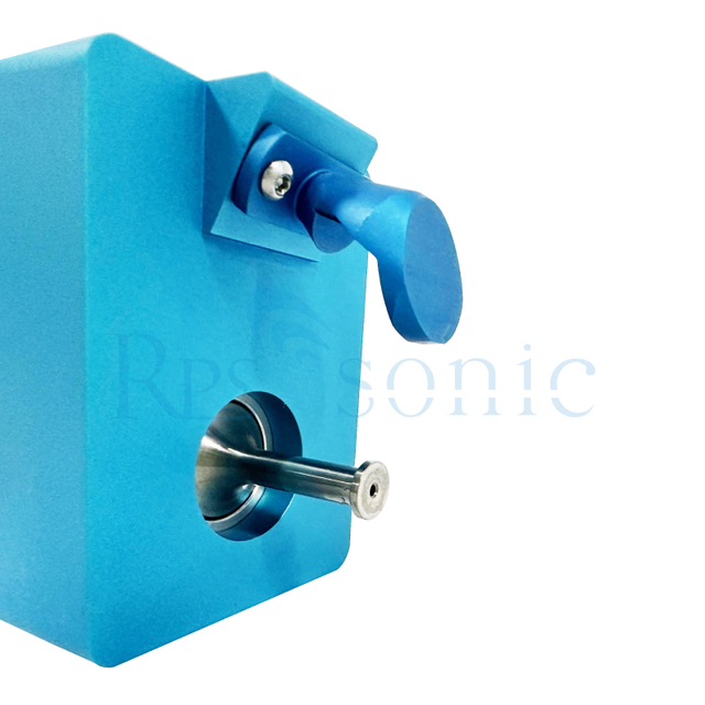
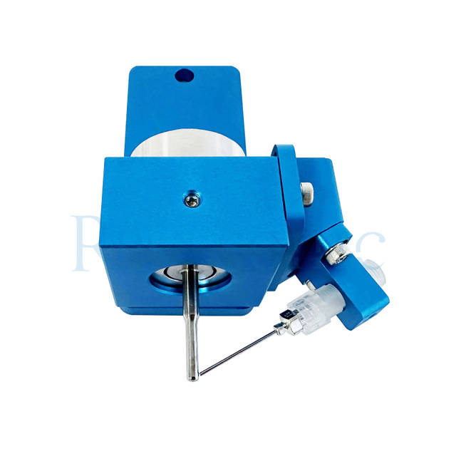
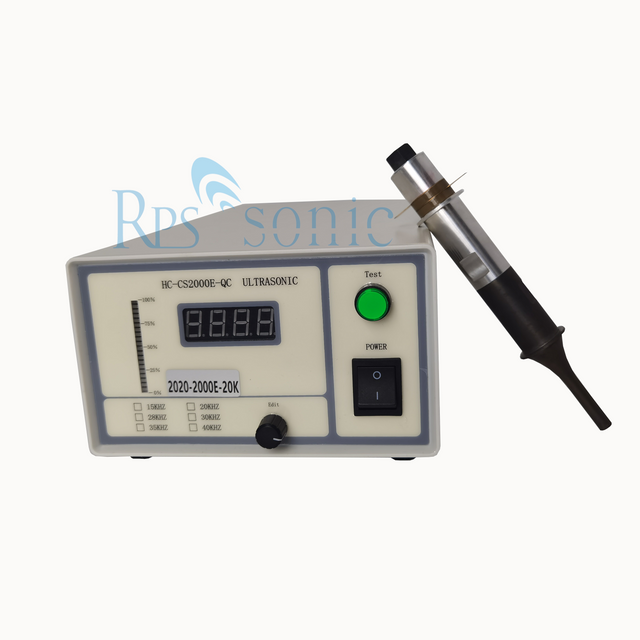
In practical applications, achieving uniformity also relies on the synergistic optimization of liquid flow rate, spraying speed, scan spacing, and substrate temperature. The ultrasonic spraying systems from RPS-SONIC utilize a layered approach, enabling precise control over the photoresist flow rate, spraying speed, and deposition amount, thereby ensuring highly uniform coatings on both planar surfaces and 3D structures. For wafers featuring microstructures, an ultrasonic spray nozzle—equipped with specialized vortex channels—converts the carrier gas into a rotating airflow. This causes the atomized droplets to be dispersed in a cyclonic pattern, which not only expands the spray coverage area but also enables the photoresist to effectively coat vertical sidewalls and tight corners. This "rotational spray" technique is particularly critical for the deep trenches and cantilever structures commonly found in MEMS devices.
A recent process study has further validated the feasibility of ultrasonic spraying for micron-scale lithography. Researchers used AZ1505 positive photoresist to deposit a film approximately 2 microns thick onto 5-inch and 12-inch substrates via ultrasonic spraying. Subsequently, a laser direct-writing system was employed to successfully transfer patterns with a resolution of 3 ± 1 microns. These results demonstrate that ultrasonic spraying is not limited to thick-film or coarse-feature applications; with optimized process parameters, it can also meet the precision requirements of micron-scale lithography.
Indispensability in Complex Topographies and Advanced Packaging
While spin-coating—with its finely tuned parameters—can achieve competitive uniformity on planar wafers, ultrasonic spraying offers unique, irreplaceable advantages when dealing with high-aspect-ratio structures or large-format panels used in advanced packaging.
In MEMS manufacturing, trenches or through-holes created by deep reactive-ion etching (DRIE) often require a continuous, thickness-controlled photoresist layer along their sidewalls. Spin-coating is largely ineffective for such topographies: the combined influence of surface tension and centrifugal force tends to pull the photoresist away from the sidewalls, resulting in accumulation at the bottom while leaving the sidewalls exposed. In contrast, the low-velocity droplets produced by ultrasonic spraying are unaffected by centrifugal force; upon landing on the sidewalls, they remain in place, accumulating layer by layer to form a conformal coating. Since the mid-1980s, Sono-Tek has utilized ultrasonic spraying for photoresist deposition on silicon wafers. Their systems deliver coverage quality unattainable via spin-coating, particularly when processing extreme topographies—such as etched V-grooves, 90-degree vertical trenches (approaching the full thickness of the silicon wafer), and glass microlens arrays. Engineering experience at Oriental Jinrong (Dongfang Jinrong) further confirms that ultrasonic spraying significantly outperforms traditional spin-coating in achieving uniform coverage within high-aspect-ratio trenches, thereby reducing device failures caused by excessive metal exposure to etchants.
The industry’s shift toward Panel-Level Packaging (PLP) has created broader application opportunities for ultrasonic spraying. In fan-out packaging, the formation of uniform photoresist patterns for Redistribution Layers (RDLs) on large, rectangular panels presents challenges for spin-coating, which suffers from severe edge effects and high material waste when applied to non-circular substrates. Because ultrasonic spraying is a non-contact process, it is independent of substrate shape; it enables the deposition of photoresist at a controlled thickness across the entire panel surface—including within vias and over circuit traces—while minimizing edge bead accumulation and streaking defects. For large-area substrates containing hundreds to thousands of individual package sites, the high transfer efficiency and closed-loop flow control inherent to ultrasonic spraying are critical for maintaining batch-to-batch consistency.
Nozzle Design: Application-Specific Adaptation and Anti-Clogging Capabilities
Photoresist spraying imposes conflicting requirements on the nozzle: it must achieve fine atomization while remaining resistant to clogging. Resins and solvents within photoresists tend to form a "skin" rapidly as they evaporate at the nozzle tip; consequently, the tiny orifices of conventional pressure-based nozzles are highly prone to clogging. In contrast, ultrasonic nozzles do not rely on pressure for atomization—the liquid is broken into droplets solely through vibration on the nozzle surface. Furthermore, the high-frequency vibration provides a self-cleaning effect, enabling the continuous spraying of photoresists with high solids content.
Nozzle configurations must also be selected based on the specific topography of the substrate. For planar wafers, conventional focusing-type nozzles deliver a narrow, high-density spray. In contrast, for substrates featuring vertical sidewalls or curved surfaces, dispersing-type nozzles utilize a rotating airflow to guide droplets, ensuring multi-angle adhesion and providing superior coverage of non-horizontal surfaces while maintaining excellent uniformity. Notably, a patented technology highlights that in contact-type ultrasonic atomization, rapid solvent evaporation—triggered by oscillations at the nozzle tip—remains a primary cause of clogging; a non-contact resonant cavity design, however, can further enhance resistance to such contamination. This development reflects the ongoing evolution of ultrasonic spraying equipment toward greater reliability.
Conclusion
In the photoresist industry, the value of ultrasonic atomization spraying lies not in the complete replacement of spin-coating, but in providing engineering solutions for scenarios where spin-coating falls short. As substrate topographies shift from planar to three-dimensional, as substrate formats evolve from wafers to large-area panels, and as photoresist costs become an increasingly sensitive factor, the low-velocity conformal deposition and high material utilization efficiency of ultrasonic spraying have transitioned from "optional advantages" to "essential capabilities." With the validation of micron-scale resolution spraying processes and the maturation of anti-clogging nozzle designs, this technology is expanding beyond niche applications in MEMS and advanced packaging into a broader range of photoresist coating scenarios, establishing itself as an indispensable tool in the lithography process toolkit.