What Is Ultrasonic Photoresist Spraying Equipment?
Views: 103 Author: Site Editor Publish Time: 2026-04-02 Origin: Site
What Is Ultrasonic Photoresist Spraying Equipment?
Ultrasonic photoresist spraying equipment is a precision coating device that uses ultrasonic atomization technology to uniformly spray photoresist (photocurable photoresist) onto the surface of a substrate for photolithography processes.
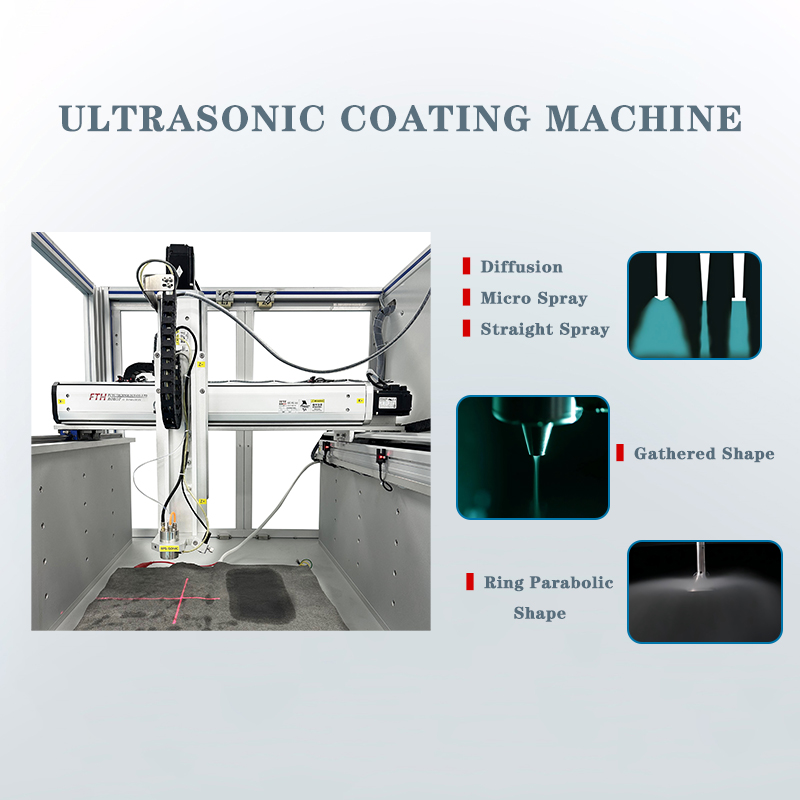
Simply put, its core working principle is: high-frequency vibrations (typically 20kHz-120kHz) generated by an ultrasonic transducer atomize liquid photoresist into micron-sized (a few micrometers to tens of micrometers) droplets. A carrier gas (such as nitrogen) then guides these droplets and uniformly deposits them onto the substrate surface, ultimately forming a uniform and dense photoresist film.
Compared to traditional spin coating, ultrasonic spraying equipment has the following significant characteristics and advantages:
Suitable for irregular surfaces: Spin coating relies on centrifugal force generated by high-speed rotation to flatten the photoresist, and can only handle flat circular or square substrates. Ultrasonic spraying does not rely on substrate rotation, making it ideal for uniformly coating non-planar and uneven surfaces such as deep trenches, three-dimensional microstructures, high aspect ratio vias, and substrates already containing microchips.
High material utilization: Spin coating typically results in a large amount of photoresist being ejected from the substrate edges, leading to significant material waste (utilization is usually only 10%-30%). Ultrasonic spraying, a "direct writing" or directional spraying process, can precisely deposit most of the photoresist onto the substrate, achieving a material utilization rate of 70%-90%. This significantly reduces costs for expensive photoresists (especially specialty photoresists used in advanced packaging or MEMS).
Highly controllable film thickness: By controlling the flow rate of the atomizing head, carrier gas pressure, and nozzle movement speed, film thickness control from submicron to hundreds of micrometers can be achieved on large-size substrates, with good uniformity.
Non-contact: The nozzle does not contact the substrate during spraying, preventing physical damage to fragile structures (such as microcantilever beams and microneedle arrays).
This equipment is mainly used in the following fields:
Advanced semiconductor packaging: Coating photoresist onto wafers with high bumps or deep holes in wafer-level packaging (WLP) and fan-out packaging.
MEMS (Micro-Electro-Mechanical Systems): Uniform photoresist coating on silicon wafers with deep cavities or complex sensor structures.
Microfluidics and Biochips: Forming a uniform photoresist layer on glass or polymer substrates.
Thick Photoresist Lithography: When photoresist layers tens or even hundreds of micrometers thick are required, multiple spray coatings are more effective than single spin coatings in achieving bubble-free, well-edge thick films.
Large or Non-Circular Substrates: Such as square glass or metal substrates in panel-level packaging (PLP).
It is important to note that ultrasonic spray coating equipment is generally more expensive than spin coating equipment, and adjusting process parameters (such as atomization power, temperature, and flow rate) is more complex. Furthermore, a "leveling" step is usually required after spray coating to eliminate the slight orange peel effect that may be caused by droplet buildup, ensuring that the final film surface flatness meets photolithography requirements.