The Application of Ultrasonic Technology in The Coating of Photoresist
Ultrasonic technology applied to photoresist coating is an advanced, precise, and highly targeted process in the microelectronics and semiconductor manufacturing fields.
Core Concept: A Paradigm Shift from "Spinning" to "Spraying"
Traditional photoresist coating primarily uses spin coating, relying on centrifugal force to spread the resist. However, its material utilization rate is extremely low (<5%), and it is difficult to handle uneven, large-sized, or three-dimensional substrates.
Ultrasonic spraying is a non-contact, additive manufacturing coating method that atomizes photoresist solution into micron-sized uniform droplets and precisely deposits them onto the substrate surface to achieve controllable film formation.
Main Advantages and Application Scenarios
Ultrasonic spraying is not intended to replace all spin coating, but rather to provide an irreplaceable solution in specific scenarios.
Application scenarios | Specific advantages and descriptions |
1. Save expensive materials | Material utilization is over 90%. For compound semiconductors (such as GaN and SiC), advanced packaging, and special, high-cost photoresists or polymers (such as polyimide) used in MEMS, the cost savings are enormous. |
2. Compatible with complex, non-standard substrates | Non-rotational, non-contact. • Patterned wafers: When the surface already has high aspect ratio structures (MEMS beams, deep trenches), spin coating can lead to uneven coverage and voids. Spray coating can achieve better sidewall and bottom coverage. • Large panels: Used in the manufacture of flat panel displays (FPDs), large sensors, and solar cells. • Curved or flexible substrates: Substrates that cannot be rotated at high speeds, such as flexible electronics and curved glass. • Fragile substrates: Ultra-thin wafers (<100µm) or fragile materials, avoiding rotational stress. |
3. Achieving special coating structures | Strong digital program control capabilities. • Gradient coating: Achieves continuous variation in film thickness within specific areas by controlling the spraying path and flow rate. • Multilayer coating: Allows sequential spraying of different types of photoresist or other functional materials (such as sacrificial layers or planarization layers) without changing equipment. • Localized coating: Precisely repairs only selected areas (such as specific regions or defects on a chip), avoiding global coating and subsequent complex etching. |
4. Uniform coating of large surfaces | For areas much larger than traditional silicon wafers (such as 8-inch or 12-inch), a precision scanning system can be used to achieve uniform control of the film thickness across the entire panel, overcoming the "edge effect" of spin coating. |
Key Technological Challenges and Solutions To achieve semiconductor-grade quality in ultrasonic photoresist spraying, the following challenges must be overcome:
Film Thickness Uniformity and Repeatability
Challenge: Achieving nanometer-level film thickness control and ±1-2% uniformity.
Solutions:
Precision Motion Control: High-precision linear motors and scanning algorithms.
Dynamic Substrate Heating: Precisely controlling the substrate temperature during spraying (typically preheating to 40-80°C) promotes rapid and uniform solvent evaporation, allowing droplets to better level and fuse on the surface, forming a smooth, defect-free film.
Closed-Loop Control System: Integrating real-time film thickness monitoring (e.g., optical interferometer) for feedback adjustment.
Defect Control
Challenges: Orange peel effect, satellite droplets, bubbles, particulate contamination.
Solutions:
Optimizing Atomization Parameters: Adjusting ultrasonic frequency, power, and solution characteristics (viscosity, surface tension) to generate a uniform and stable droplet flow.
Solvent Engineering: Using mixed solvent systems to balance drying speed and leveling ability. Cleanroom Environment: Operate in an ISO Class 5 (or higher) cleanroom equipped with a high-efficiency particulate filtration system.
Compatibility with Subsequent Photolithography Processes
Challenge: The initial state of the photoresist film formed by spray coating (solvent residue, molecular arrangement) may differ from that of spin coating, affecting subsequent processes such as exposure and development.
Solution: A systematic redevelopment and optimization of the entire photolithography process parameters is required, including pre-baking (soft bake) conditions, exposure dosage, post-baking (PEB) temperature and time, developer formulation, and development time.
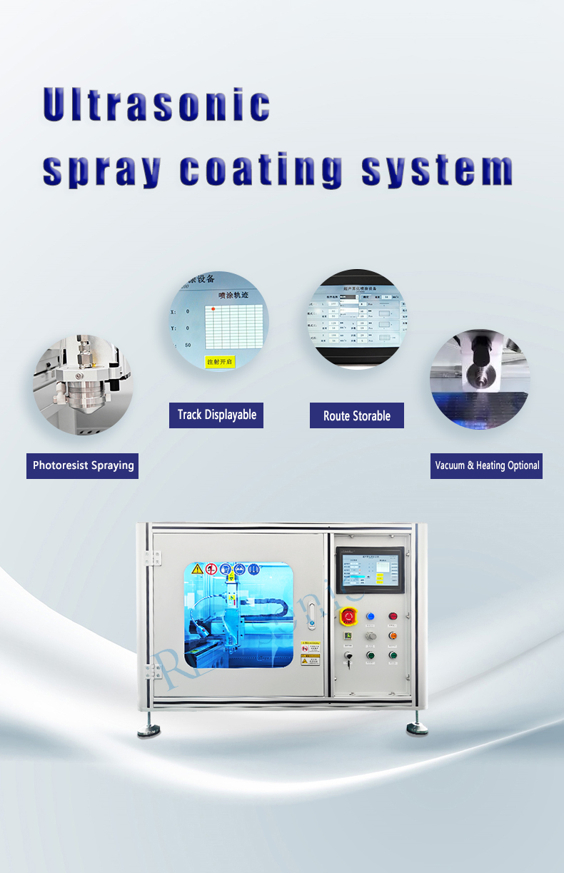
Typical Process Flow
Substrate Pretreatment: Cleaning, dehydration, drying, and coating with a tackifier (such as HMDS).
Spray Preparation: Dilute the photoresist to a suitable viscosity with an appropriate solvent and filter. Fix the substrate on a heated precision motion platform.
Dynamic Spraying: Start heating the substrate to the set temperature.
The ultrasonic nozzle scans along a preset path, simultaneously atomizing and spraying photoresist droplets.
The droplets impact the heated substrate, the solvent evaporates instantly, and the colloid solidifies into a film.
Post-processing: Performs a series of photolithography steps including standard pre-baking, exposure, post-baking, development, and inspection.
Industry Application Status and Development
Main Application Areas:
MEMS Device Manufacturing: One of the preferred technologies for coating high aspect ratio structures.
Compound Semiconductors and Power Devices: Saves materials on expensive substrates such as GaN-on-SiC and GaN-on-Si.
Advanced Packaging: Used for polymer coating in Fan-Out and 2.5D/3D packaging, such as redistribution layers and under-bump metallization layers.
Photonic Integrated Circuits and LEDs: Coating on non-planar structures.
Flat Panel Displays and Flexible Electronics: Uniform coating on large-size, flexible substrates.
Development Frontiers:
Nanoparticle Suspension Spraying: Used for functional layers such as quantum dots and metal nanowires.
Multi-Material Heterogeneous Integration: Precisely sprays multiple materials with different properties onto the same substrate.
Summary
The application of ultrasonic technology in photoresist coating represents an evolution from traditional "subtractive" manufacturing (wasteful spin coating) to precise "additive" manufacturing. It perfectly solves the three core pain points of material cost, substrate compatibility, and coating of complex structures. Although there are still process challenges to overcome in the pursuit of ultimate uniformity, it has become an indispensable advanced coating tool in fields beyond Moore's Law (MEMS, packaging, heterogeneous integration) and special semiconductor manufacturing, driving the development of microelectronic devices towards more complex and diversified directions.
item | Traditional methods | ultrasonic spraying technology |
Coating uniformity | Average, prone to orange peel and dripping | Excellent, nanometer-level precision control. |
Material utilization rate | Low (30%-60%) | High (>90%) |
Impact on workpiece | May cause damage due to high pressure or liquid impact. | Non-contact, gentle, and non-damaging. |
Complex shape coverage | Poor, many blind spots | Excellent, good shape retention |
Process controllability | Low | Extremely high, digital programming control |
Coating thickness | Thicker, harder to control | Ultra-thin, with precision down to the submicron level |
V. Applications and Future Prospects
Current Applications: Primarily used in the manufacture of high-end endoscopes such as disposable duodenoscopes, bronchoscopes, and colonoscopes, as well as the remanufacturing and repair of reusable endoscopes.
Future Trends:
Multifunctional Composite Coatings: Multiple layers of coatings with different functions are sequentially sprayed onto the same surface (e.g., antireflective coating followed by hydrophobic coating).
Intelligentization and AI Integration: Utilizing machine vision to automatically identify the spraying area and optimizing the spraying path and parameters through AI algorithms.
New Material Development: Such as "self-healing" coatings that automatically repair minor scratches; or drug-loaded coatings that release therapeutic drugs during examination.
In conclusion, ultrasonic spraying technology for semiconductor endoscopes is one of the key manufacturing processes ensuring the high performance, high reliability, and safety of modern precision medical endoscopes, and is a jewel in the crown of high-end medical device manufacturing.