How Ultrasonic Atomization Spraying Can Rebuild The Precision Limits of Surface Manufacturing
Views: 110 Author: Site Editor Publish Time: 2026-01-22 Origin: Site
How Ultrasonic Atomization Spraying Can Rebuild The Precision Limits of Surface Manufacturing
Traditional coating technologies are facing unprecedented challenges: as chip feature sizes approach the nanoscale, as flexible electronic devices require uniform film formation on highly curved surfaces, and as every precious drop of new functional material cannot be wasted—a non-contact additive manufacturing technology called "ultrasonic atomization spraying" is quietly rewriting the rules of surface coating. It atomizes solutions such as photoresist into micron-sized uniform droplets and precisely deposits them onto the substrate surface, achieving a paradigm shift from "covering" to "programming." This technology is not only a revolutionary leap beyond traditional spin coating and spraying, but also an acoustic key to unlocking the next generation of precision manufacturing.
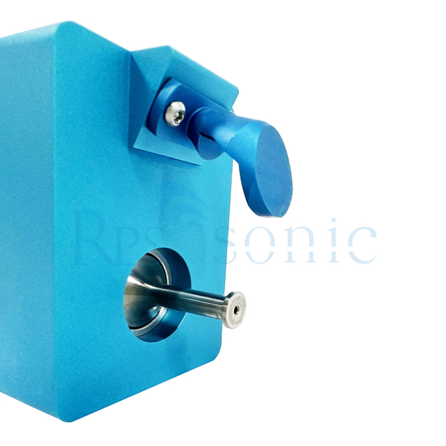
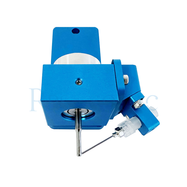
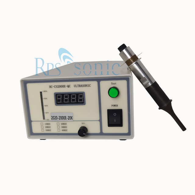
The core principle of ultrasonic atomization spraying is a "quiet storm" occurring at the nozzle tip. Unlike traditional pressure spraying, which relies on high-speed airflow to tear the liquid film, ultrasonic spraying utilizes high-frequency mechanical vibrations (typically between 20 kHz and 200 kHz) generated by piezoelectric transducers to directly transfer energy to the liquid layer. When vibrational energy overcomes the surface tension of a liquid, the solution forms tiny ripples called "capillary waves" on its free surface, ejecting micron-sized droplets with uniform size and near-zero initial velocity from the wave crests. This "gentle generation" mechanism avoids splashing and rebound caused by high-speed impacts, forming the physical basis for achieving ultrathin, uniform, and defect-free films.
This unique atomization method gives ultrasonic spraying unparalleled process advantages. First, it offers superior uniformity and controllability. The droplet size distribution is extremely narrow (relative standard deviation can be less than 10%), and the deposition process can be precisely controlled by programming the path, flow rate, and number of layers, achieving sub-micron-level film thickness control and maintaining excellent consistency even on complex three-dimensional surfaces. Second, it offers extremely high material utilization and adaptability. Non-contact spraying can deposit over 90% of the material onto the target substrate and is compatible with almost any pumpable liquid—from traditional photoresists to expensive perovskite precursor solutions, graphene dispersions, and even bioactive coatings. Finally, it is friendly to heat-sensitive and flexible substrates. The room-temperature, low-pressure deposition environment perfectly avoids thermal damage and mechanical stress, making it possible to manufacture electronic devices on plastics, paper, and even textiles.
In the semiconductor and display industries, ultrasonic spraying is becoming a key breakthrough in overcoming the bottlenecks of spin coating. In applications such as preparing large-area uniform photoresist coatings, depositing OLED thin-film encapsulation layers, and fabricating microlens arrays, it not only solves the problems of edge removal and material waste in spin coating but also enables real-time online thickness monitoring and closed-loop control. In the new energy field, this technology is used for the uniform coating of fuel cell catalyst layers, perovskite solar cell functional layers, and lithium battery electrode materials, directly affecting the conversion efficiency and cycle life of devices. Even in the biomedical field, ultrasonic spraying can construct bioactive coatings or drug-releasing layers on implant surfaces in a cell-friendly manner.
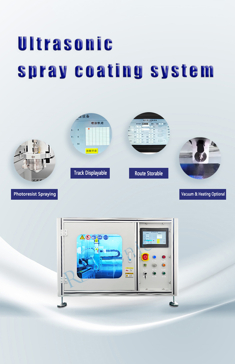
The technological frontier is evolving towards "intelligent acoustic deposition." Next-generation systems, through the integration of multi-axis motion platforms, machine vision positioning, and online spectral film thickness monitoring, achieve a true "perception-decision-execution" closed loop. Adaptive algorithms can adjust the spraying path and parameters in real time according to the substrate morphology; multi-nozzle array technology enables large-area, efficient, and parallel processing; and precise electronic control of droplet size and velocity makes "programmable droplet landing point" a reality. These evolutions are elevating ultrasonic spraying from a coating tool to a digital additive manufacturing platform.
Looking to the future, with the booming development of the Internet of Things, flexible electronics, and sustainable manufacturing, the demand for precise, efficient, and adaptable surface manufacturing technologies will grow exponentially. Ultrasonic atomization spraying technology, with its unique non-contact, low-loss, high-uniformity, and excellent adaptability, not only has the potential to replace traditional coating processes in more fields, but may also give rise to entirely new product forms and manufacturing paradigms—for example, directly "printing" functional circuits on complex curved surfaces, or constructing gradient functional materials at the microscale.
When high-frequency sound waves agitate precise ripples on a liquid surface, what emerges is no longer ordinary droplets, but "digital raindrops" for building future devices. Ultrasonic atomization spraying technology, with its silent vibrations, is depicting a clear trajectory of macro-industrial transformation in the microscopic world, reshaping the precision limits and imagination boundaries of human beings in functionalizing surfaces.
item
Traditional methods
ultrasonic spraying technology
Coating uniformity
Average, prone to orange peel and dripping
Excellent, nanometer-level precision control.
Material utilization rate
Low (30%-60%)
High (>90%)
Impact on workpiece
May cause damage due to high pressure or liquid impact.
Non-contact, gentle, and non-damaging.
Complex shape coverage
Poor, many blind spots
Excellent, good shape retention
Process controllability
Low
Extremely high, digital programming control
Coating thickness
Thicker, harder to control
Ultra-thin, with precision down to the submicron level
V. Applications and Future Prospects
Current Applications: Primarily used in the manufacture of high-end endoscopes such as disposable duodenoscopes, bronchoscopes, and colonoscopes, as well as the remanufacturing and repair of reusable endoscopes.
Future Trends:
Multifunctional Composite Coatings: Multiple layers of coatings with different functions are sequentially sprayed onto the same surface (e.g., antireflective coating followed by hydrophobic coating).
Intelligentization and AI Integration: Utilizing machine vision to automatically identify the spraying area and optimizing the spraying path and parameters through AI algorithms.
New Material Development: Such as "self-healing" coatings that automatically repair minor scratches; or drug-loaded coatings that release therapeutic drugs during examination.
In conclusion, ultrasonic spraying technology for semiconductor endoscopes is one of the key manufacturing processes ensuring the high performance, high reliability, and safety of modern precision medical endoscopes, and is a jewel in the crown of high-end medical device manufacturing.