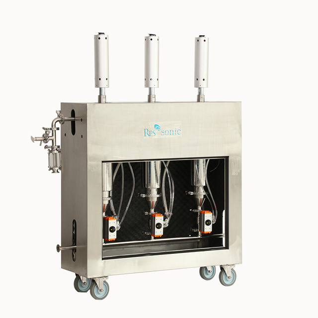
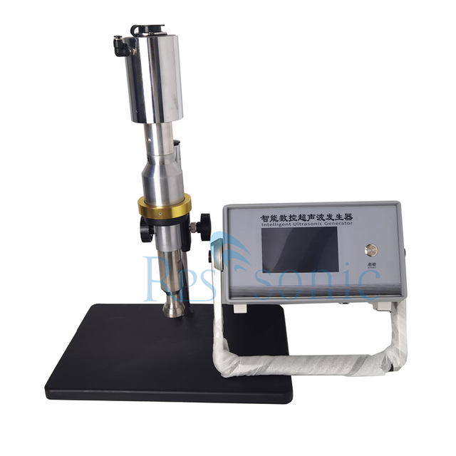
Ultrasonic Cleaning Equipment for The Semiconductor Industry: Wafer, Silicon Slice, And Precision Component Cleaning Solutions
In semiconductor manufacturing, cleanliness directly impacts product yield, reliability, and the stability of subsequent processes. From silicon wafers and processed wafers to packaging substrates, metal parts, quartz components, and production fixtures, many components generate particles, metallic contamination, organic residues, and other microscopic contaminants during processing.
As semiconductor manufacturing advances toward smaller feature sizes, higher integration, and greater precision, traditional manual cleaning and simple spray cleaning methods increasingly struggle to meet the requirements for precision cleaning.
**Ultrasonic cleaning equipment** utilizes high-frequency sound waves to induce acoustic cavitation within the cleaning fluid. The formation and collapse of countless tiny bubbles generate microscopic shockwaves, fluid agitation, and acoustic streaming, thereby facilitating the removal of contaminants adhering to the workpiece surface.
For semiconductor components and process steps suitable for ultrasonic treatment, ultrasonics serve as a vital component of the precision cleaning process.
What is semiconductor ultrasonic cleaning?
Semiconductor ultrasonic cleaning is a technique that employs ultrasonic energy to enhance the removal of contaminants from workpiece surfaces by the cleaning fluid.
When ultrasonic waves enter the cleaning fluid, a multitude of tiny cavitation bubbles are generated.
These bubbles undergo a continuous cycle of:
Formation → Growth → Collapse
The collapse of these bubbles produces localized micro-jets and intense fluid agitation, helping to break the adhesive bonds between contaminants and the workpiece surface.
For complex structures, tiny pores, and areas difficult to access directly, the acoustic streaming generated by ultrasonic waves helps the cleaning fluid penetrate these regions.
The basic process can be outlined as follows:
Ultrasonic Generator
↓
Ultrasonic Transducer
↓
Acoustic Cavitation in Cleaning Fluid
↓
Reduction of Adhesion between Contaminants and Workpiece Surface
↓
Detachment of Particles, Oil, and Residues
↓
Rinsing / DI Water Cleaning
↓
Drying
Why does the semiconductor industry require high-precision cleaning?
Various contaminants may be present in the semiconductor production environment. Examples:
Particulate contamination
Includes:
· Micro-particles
· Dust
· Machining debris
· Process-generated residue particles
Organic contamination
Examples:
· Oil/grease
· Photoresist-related residues
· Organic compounds
· Adhesive residues
Metallic contamination
Includes metal ions and metal particles generated or transferred during processing.
Chemical residues
Certain wet processes may generate chemical residues that require removal through subsequent cleaning and rinsing steps.
In advanced semiconductor manufacturing, contamination control strategies must be designed based on specific processes, materials, and cleanliness requirements.
Therefore, semiconductor cleaning is not merely about "washing parts clean"; it requires establishing a comprehensive process system comprising:
Cleaning → Rinsing → Ultrapure water cleaning → Drying → Contamination control.
The Core Principle of Ultrasonic Cleaning: Acoustic Cavitation
The most critical mechanism in ultrasonic cleaning is acoustic cavitation.
When high-frequency ultrasonic waves are applied to a liquid, they generate a rapidly fluctuating pressure field.
In regions of negative pressure, tiny bubbles may form within the liquid.
As the sound waves continue to act, these bubbles expand and contract repeatedly before eventually collapsing rapidly.
The localized micro-jets and turbulence generated by bubble collapse act upon the surface of the workpiece.
This enables ultrasonic cleaning to effectively clean:
· Flat surfaces
· Grooves
· Holes and apertures
· Fine structures
· Surfaces with complex geometries
Consequently, compared to simple liquid immersion, ultrasonics significantly enhance the interaction between the cleaning fluid and contaminants.
Why Is Controlling Ultrasonic Parameters Essential for Semiconductor Cleaning?
Higher ultrasonic power is not necessarily better.
For standard industrial parts, high-intensity cavitation often enhances cleaning effectiveness.
However, for precision semiconductor components, excessive acoustic energy can increase the risk of:
· Surface damage
· Microstructure damage
· Material erosion
· Contaminant redeposition
Therefore, comprehensive control of the following factors is required:
Frequency + Power density + Time + Temperature + Cleaning fluid + Workpiece structure
Advantages of Ultrasonic Cleaning Equipment
For semiconductor components suitable for ultrasonic processing, the technology offers the following benefits:
Deep cleaning:
Acoustic cavitation allows the cleaning fluid to penetrate complex structures and hard-to-reach areas.
Reduced manual labor:
Can be integrated with automated robotic systems.
Controllable parameters:
Frequency, power, time, and temperature can all be regulated.
Suitable for batch processing:
Large cleaning tanks can process multiple workpieces simultaneously.
Multi-tank process capability:
Cleaning, rinsing, and drying processes can be combined.
Customizability:
Equipment can be designed according to workpiece dimensions and production cycle requirements.
Conclusion
Ultrasonic cleaning equipment is a key technology in the field of precision semiconductor component cleaning.
From quartz components and precision metal parts to wafer carriers, production jigs, and certain packaging components, the acoustic cavitation and acoustic streaming generated by ultrasonics enhance the microscopic action of the cleaning fluid, effectively removing particles, oils, and processing residues suitable for this method. However, the semiconductor industry demands exceptionally high standards for cleanliness and surface integrity; therefore, equipment design should not simply aim for higher ultrasonic power. Instead, a comprehensive design approach is required, taking into account factors such as workpiece material, contaminant type, cleaning fluid, frequency, power density, cleaning duration, and target cleanliness levels.
For advanced wafers and microstructured devices, it is also necessary to evaluate the suitability of conventional ultrasonic, megasonic, and other cleaning technologies based on specific process requirements.
By integrating ultrasonic cleaning, DI water rinsing, precision filtration, temperature control, automated robotic handling, and clean drying, it is possible to construct automated precision cleaning systems tailored to various stages of semiconductor manufacturing.